
My latest posts can be found here: Previous blog posts:
Additionally, some earlier writings: |
Way back in the 70s when I was building logic circuits, I was
warned repeatedly that I'd have to get a few things right, or
risk "locking up" or "burning out" the CMOS chips I was using.
The bogeyman was "Signal Reflection", but no one could tell me
what it was, or why it was so bad.
The Context: CMOS(Skip this section at first if you like, you can return to it later if you want more of the details.) It's still true today that all logic chips (with a few but very significant exceptions) use the Field Effect Transistor, or FET. You can go to Wikipedia and read more about that than you ever wanted to know, but the basic idea is this. We take a crystal of pure silicon (other substrates are available) and carefully diffuse tiny amounts of impurities in very specific patterns. Advances in semiconductor physics allow us to cram ever more transistors (electrically-controlled switches, essentially) onto a single chip of silicon.
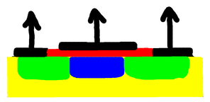
Some of these contaminants have an extra electron, and some have one less electron. In green we've marked a channel where there's a lot of extra electrons. As a result, the green channels conduct electricity without too much resistance. The blue section is where there is very little contaminant.
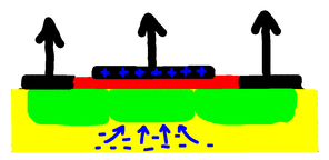
Now let's remove electrons from the metal plate. That makes it positively charged, attracting electrons from the surrounding silicon into the blue area. That, in turn, provides enough extra electrons to convert it from being semi-conducting to being properly conducting. Thus we can now have current flowing between the green channels. It becomes conducting.
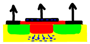
So by putting a positive voltage on the plate the outer connections are connected, as if by a switch, and by putting a negative charge on the metal plate we effectively turn the switch off, isolating the contacts. And thus we have a switch, controlled by a voltage. By using different contaminants we can change the characteristics, having it turn on with a negative charge instead of a positive one, and off with a positive charge instead of a negative one. The elements boron, arsenic, phosphorus, and occasionally gallium are used to dope (contaminate) the silicon. Combining the different types allows us to create all sorts of gates, and hence combinatorial circuits. You can read a little more about this here:
So what's the problem?Firstly, you'll notice that the "gate" is turned on and off by putting a very small charge on a very small metal plate. It really doesn't take much charge at all, and the input has a very high impedance ... it has a very high resistance to current flow. So in a sense, it's like the end of a wire. Secondly, early circuits made with this technology had effectively no protection against static charge or over-voltage. If you walked on a carpet and then picked up a chip, very likely you'd fry its delicate internals, rendering it useless. So you had to employ all sorts of anti-static measures. Thirdly, you had to design your circuit not to have over-voltages, and this is where "Signal Reflection" comes in. I'm not going to go over all the ins and outs of circuit design, most of the concerns are now over five decades out-of-date, but Signal Reflection is a nice thing to know about.
75-Ohm cableI remember hooking up a television, again, back in the 70s, and we had to change the cable connecting the aerial, because it was 75-Ohm, and we needed to use 300-Ohm. I was confused. It was wire, and certainly if you connected a meter to measure the resistance, you didn't get 75 Ohms, or 300 Ohms. You got effectively 0 Ohms. It was wire, after all, and wire didn't have resistance. No, but it has impedance. When you have a current flowing down the wire, you have electrons in motion (although not as much as you may think!). And if you have a moving charge, you have a magnetic field. So when you start the current, it starts to create the magnetic field, and a changing magnetic field creates a voltage in the opposite direction. So that opposes the current, giving a dynamic resistance. So starting the current off down the wire causes a resistance, and we can then talk about how much resistance we experience. That depends on a lot of things, but it serves to show that even just current on a wire is a complex thing.
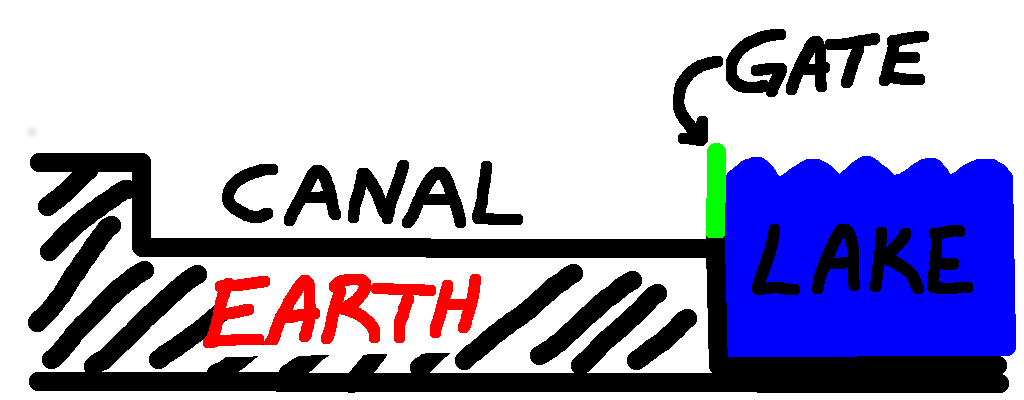
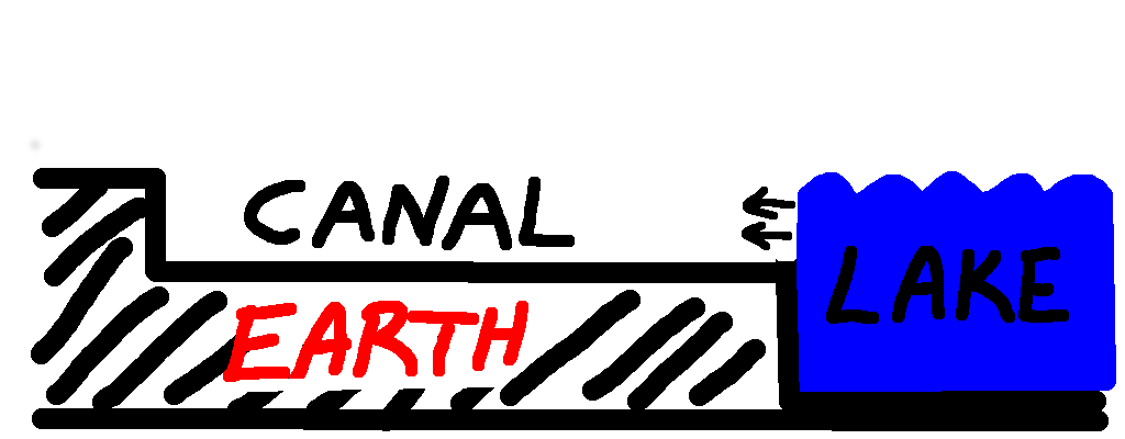
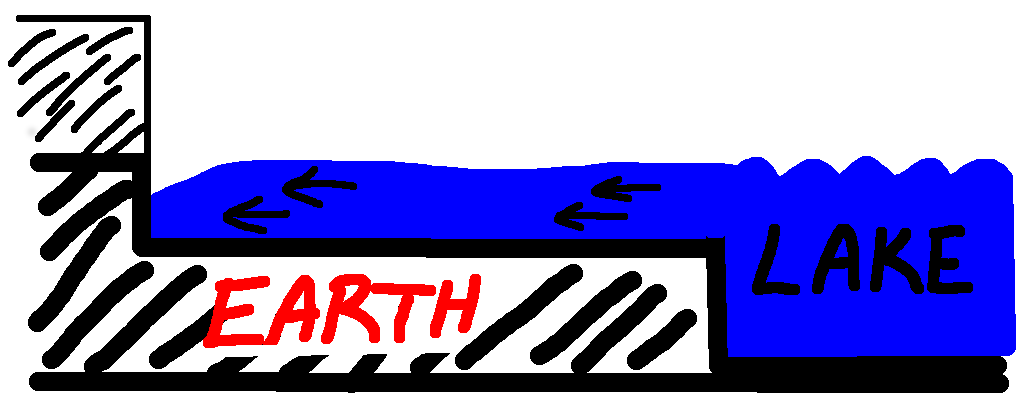
Water down a canalLet's suppose we have a lake, and we've just constructed a canal. We haven't yet connected the canal to the lake, but we're about to break through and let water in for the first time. The canal is only about a kilometre long, but we're looking forward to water-based activities on this stretch.
So here we are, ready to open the gate and let the water flow into the canal for the first time. In the diagram we have magically vanished the gate.
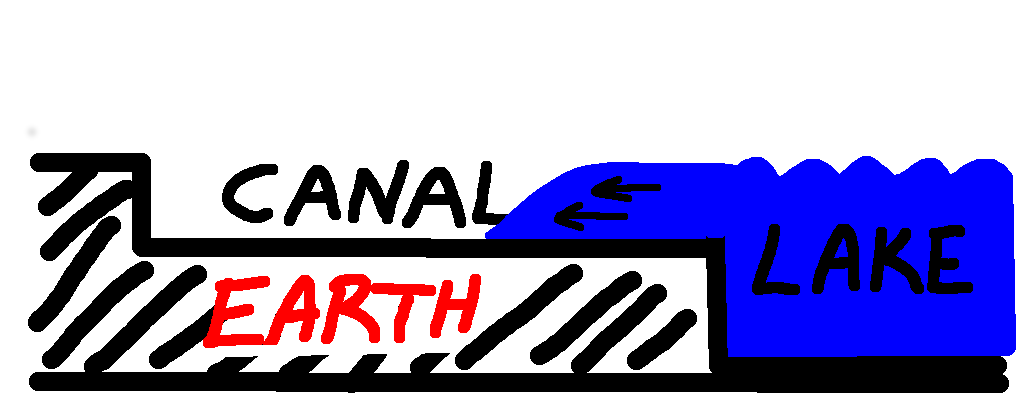
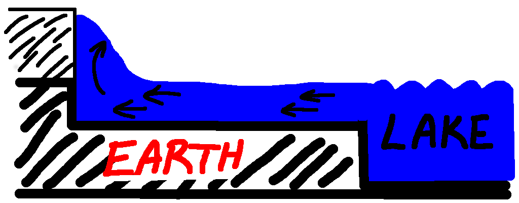
So water starts flowing along the canal. It takes some time to get there, and we've pictured here the water as it's about halfway along, supplied by the vast lake behind, flowing into the void ahead.
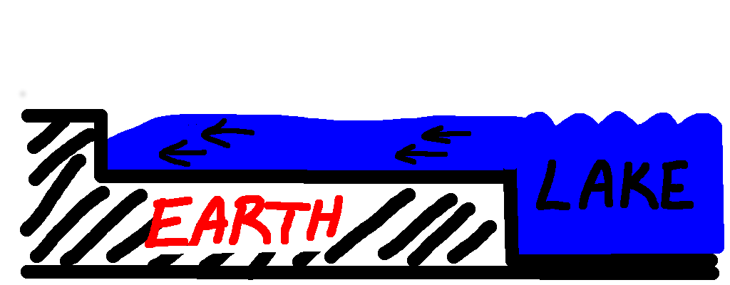
Now it reaches the end, and the canal is full. But there a problem.
The water further back, close to the lake, doesn't "know" that the canal is full. The water in the canal is still flowing, and there is no reason for it to stop. So it just keeps flowing ...
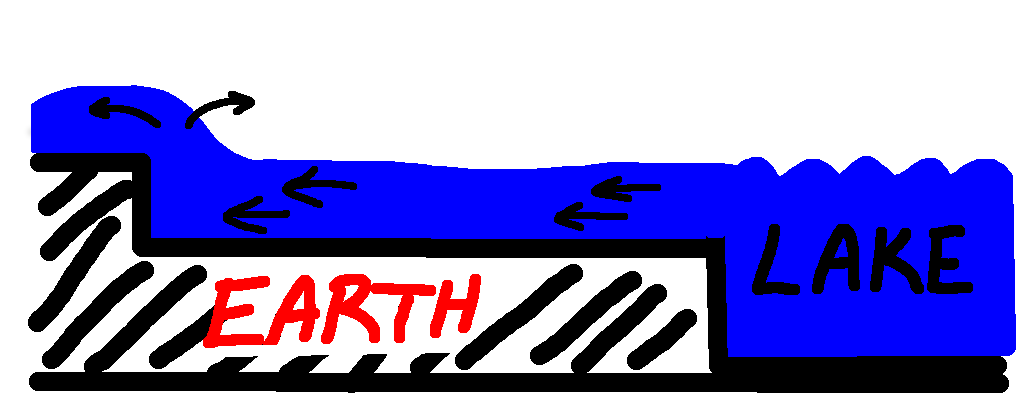
And as you can see, it will spill over the end, which could be quite amusing for those watching, but less amusing for anyone caught up in the result mini-tsunami. So we need to build the end of the canal higher. What if we do that?
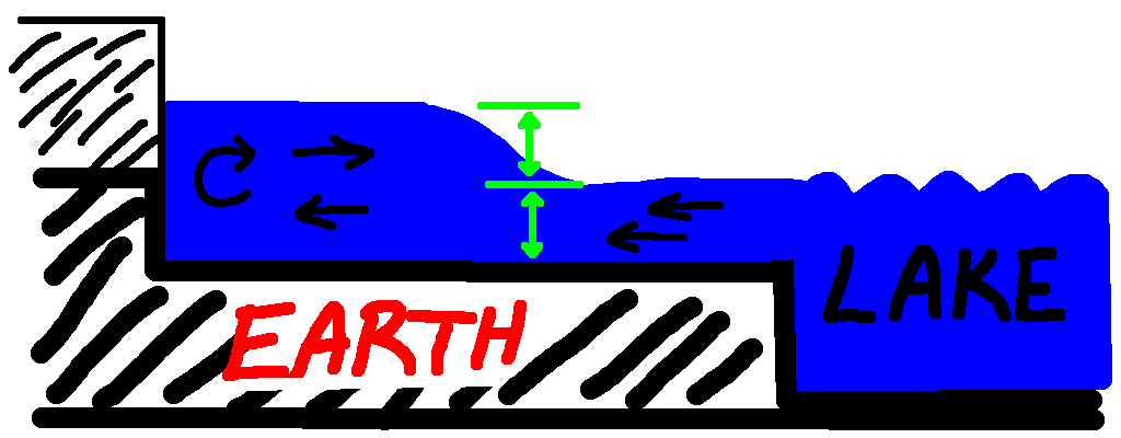
Now the water reaches the end, but the water in the canal keeps pushing, and the water at the wall will pile up. We can compute how high it will go, but there is a neat way to think about it.
The water flowing back has to "cancel out" the water flowing forward. So the height of the return wave has to be the same as the depth of the canal.
So what has all this to do with CMOS and electronics?
Electrical signal reflectionIn the specific case I was working with, I was putting a signal down a wire into the input of a CMOS gate. Now, a CMOS gate input is very like a blocked off canal. You send a current down a wire into that input, the current has nowhere to go. But the current in the wire, back at the signal origin, doesn't know that. The magnetic field around the wire works to keep the electrical current flowing, just as the weight of water in the canal keeps the water flowing. And the electrical charge at the CMOS input gate keeps piling up, just like the water at the end of the canal. And without protection, that charge spills out and into the delicate internals of the chip. At worst this will fry the components and kill it. At best the overspill can cause a lockup of the implicit parasitic transistors, and powering the entire circuit down and leaving it alone for 5 minutes to let the charge dissipate will cover it. Even so, you need to prevent the over-voltage.
Somewhere to goOne way is to give the charge/current somewhere to go. This can be done by connecting a resistor between the CMOS input gate and ground. As the current arrives, some will still be reflected back, while some will "go to ground", and you can computer the values to ensure that the voltage on the input never exceeds the maximum. Another is to connect a zener diode, still others are to put resistors elsewhere. And so on. There are books with entire chapters on this sort of stuff, and I can't do justice to the topic here. But the visualisation of water in the canal, flowing until it's stopped by a back potential, is what gave me an understanding of what signal reflection is, and how it can be prevented. Or at least, controlled.
Electricity is not waterElectricity is not water, and water is not electricity, but the analogy is good enough to provide an intuition that's not too misleading. Water analogs to electrical components can be designed, and can be made to be reasonably accurate. Wikipedia has an article on this (no surprise there): Personally, I don't like the closed pipe analogy, I prefer the open canal analogy. Voltage is the depth of water, etc. Electricity is not water ... I know ... but this analogy helped me to understand signal reflection, which we get at every change of impedance, including high to low (a narrow canal into a wider one, what kind of signal gets reflected then?) Perhaps you found this enraging, or perhaps enlightening. Or perhaps just "Meh". Let me know.
Send us a comment ...
|

 Suggest a change ( <--
What does this mean?) /
Send me email